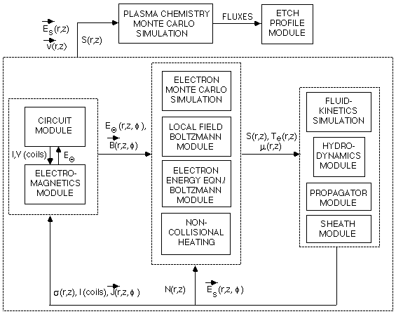

Inductively Coupled Plasmas (ICPs) are
used for high plasma density (10^11-10^12 cm-3), low gas pressure (5-20
mTorr) reactive ion etching of semiconductors for microelectronics
fabrication. ICP reactors have the desirable feature of being able to
separately control the flux and the energy of ions incident onto the
wafer. The CODPG has developed a state-of-the-art simulator called the
Hybrid Plasma Equipment Model (HPEM). The HPEM is being used by industry
to design ICP reactors which etch more uniformly and more efficiently.

The HPEM is available for transfer to industry.
The HPEM has been used to design advanced plasma equipment for 300 mm wafers. An example of one such design is shown below where an Ar/Cl2/BCl3 gas mixture at 10 mTorr is used to etch a poly-Si wafer. We show here the density of chlorine ions in the reactor.

Fig. 1 -
A conceptual design of an Inductively Coupled Plasma etching
reactor for 300 mm wafers has been performed. In the sequence
of images which follow, the operating conditions are a
gas mixture of Ar/Cl2/BCl3 = 1/1/1 at 10 mTorr pressure.
The power deposition by the inductively coupled field is
600 W with a 100 V bias applied to the substrate. The
etching process is for poly-silicon.

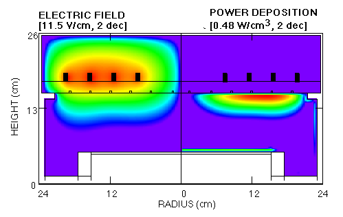
Fig. 2 -
Electric field and power deposition. The short skin depth
confines the electric field near the coil. Capacitive
coupling produces ion acceleration into the wafer.

Fig. 3 -
Chlorine ions are the dominant charged species.

Fig. 4 -
Chlorine atoms are the major etching species of the poly-Si.
They produce an etch product of SiCl2.

Fig. 5 -
Some of the etch product is reionized as SiCl2+ and SiCl+
and accelerated into the wafer. BCln+ ions are also
plentiful.
One of the issues that the CODPG has investigated using the HPEM is the effect on plasma properties of substrate structures under the wafer. These structures are, for example, cooling channels or "poles" of electrostatic chucks. We have simulated the effect of subwafer dielectrics on the plasma potential in ICP etch tools. An animation of the plasma potential during the rf cycle in such an etch tool follows.

For a copy of this simulation, please contact
Mark Kushner.