

Penetration of Plasma Into the Wafer-Focus Ring Gap in Capacitively Coupled Plasmas*
Natalia Yu. Babaeva and Mark J. Kushner
Department of Electrical Engineering & Computer Science
University of Michigan, Ann Arbor, MI 48109
1. Introduction
In plasma etching equipment for microelectronics fabrication, wafer terminating structures such as focus rings (FR) are used to make the reactant fluxes uniform to the edge of the wafer. There is an engineered gap between the edge of the wafer and the FR, typically hundreds of microns to a few mm, to provide mechanical clearance. Plasma generated species can penetrate into this gap and under the beveled edge of the wafer, depositing films and possibly creating particles. If the energy of the ions penetrating into the wafer-focus ring gap (WFG) are high enough and at critical angles, erosion of the substrate and FR may occur. In this computational investgiation, we found that the penetration of plasma into the gap and under the wafer bevel increases as the size of the gap approaches and exceeds the Debye length in the vicinity of the gap.
2. Description of the Model
The model used in this investigation, nonPDPSIM, is a multi-fluid hydrodynamics simulation in which transport equations for all charged and neutral species, Poisson’s equation and a surface kinetics model are integrated as a function of time. The fundamental equations solved in nonPDPSIM for charged particle transport are the continuity equation for species densities, Poisson's equation for the electric potential and charge densities on and inside materials. The fluxes of ions are obtained by solving the ion momentum equation. An unstructured mesh is used to resolve a dynamic range of 100-1000 to enable the reactor as well as the WFG to be accurately represented. Simulations were performed for an Ar/CF4 mixture. A relatively simple surface and bulk reaction mechanism was chosen that captures the major effects of radicals generation and possible deposition in an electronegative gas mixture. To compute ion energy and angular distributions (IEADs) to surfaces, a Plasma Chemistry Monte Carlo Module (PCMCM) was developed for nonPDPSIM. In the PCMCM, pseudo-particles representing ions and neutrals are launched from sites in the reactor. Monte Carlo techniques are used to advance their trajectories in time varying electric fields while accounting for elastic and inelastic collisions. The energy and angles of particles as they strike surfaces are recorded to provide a time averaged IEAD.
3. Plasma and Radical Penetration into the Wafer-Focus Ring Gap
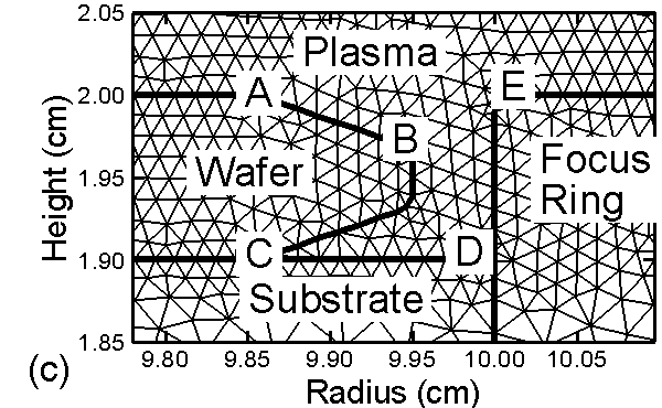
The substrate of the reactor, schematically shown in Fig. 1a, is metal and powered. The focus ring is a dielectric with negligible conductivity. The wafer has a high conductivity. An example of cycle averaged CF3+ ion density is shown in Fig. 1b and a close up of the wafer-focus ring gap is in Fig. 1c. The unstructured mesh has multiple refinement zones to gradually resolve the small dimensions of the gap.


|
| Fig. 1: Schematics of the geometry. (a) Full geometry showing the location of the wafer-focus ring gap and CF3+ ions averaged over the rf cycle for the conditions Ar/CF3=97/3, 90 mTorr, 300 V, 10 MHz (c) a close up of the wafer-focus ring gap. |
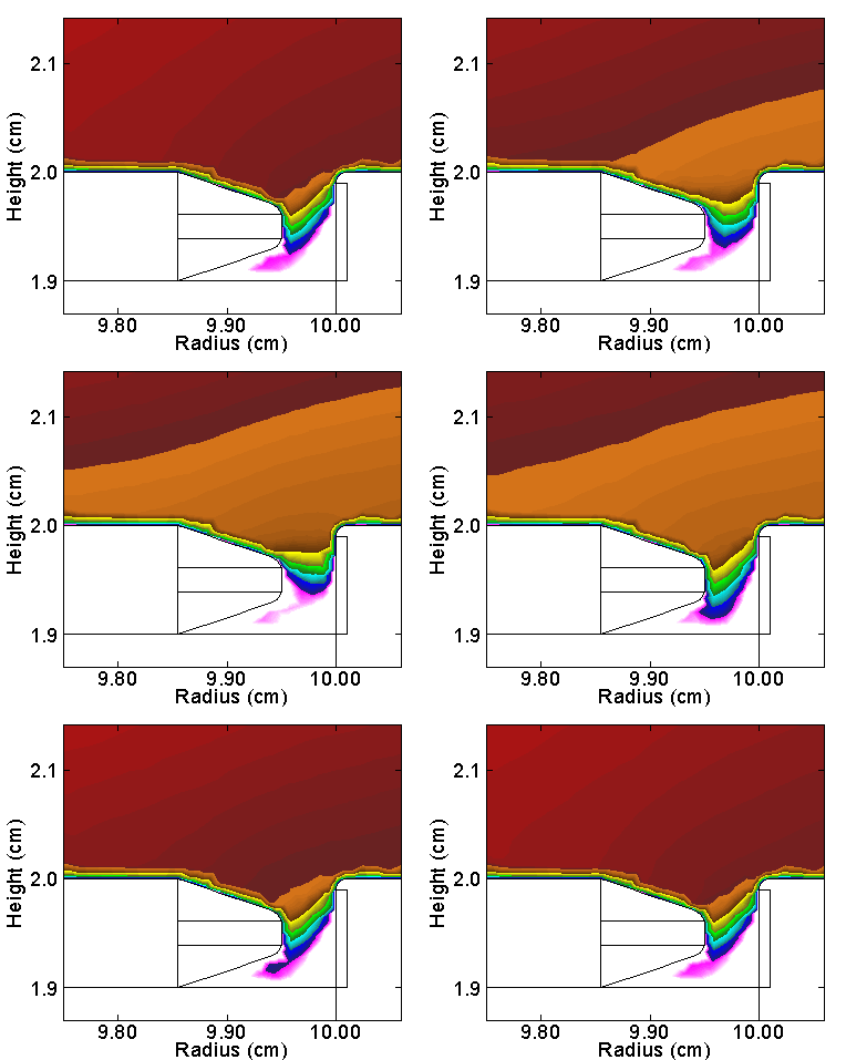
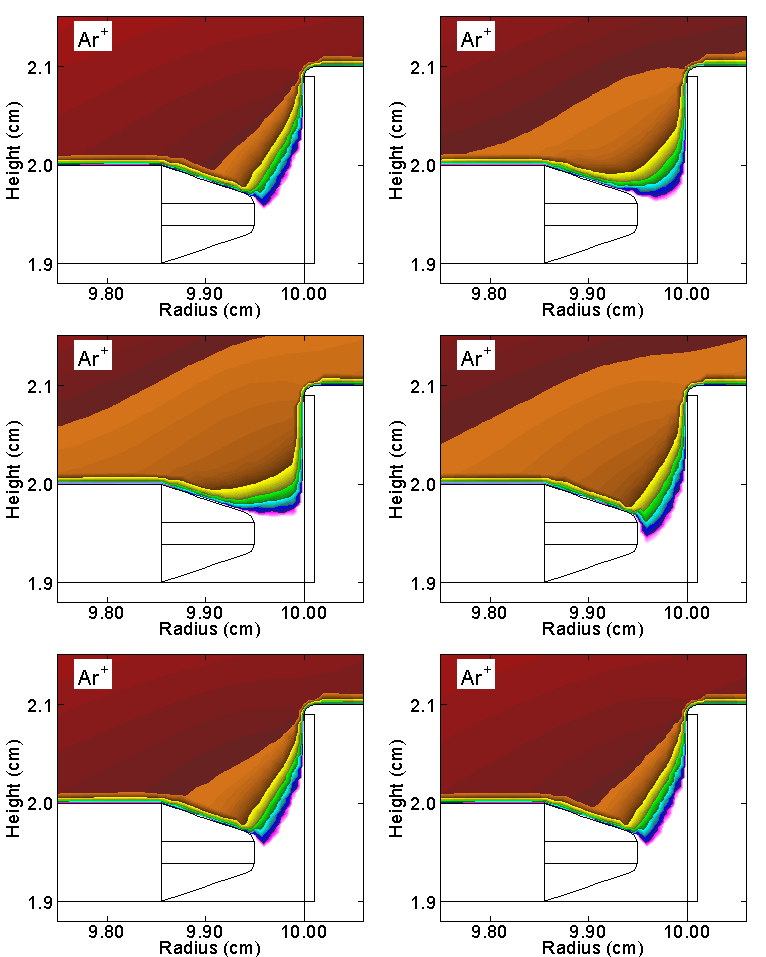
The penetration of plasma into the wafer-focus ring gap depends on the size of the gap relative to sheath thickness or Debye length and the height of the focus ring relative to the substrate. The Ar+ density during the rf cycle for the conventional and high focus ring is shown in Fig. 2a. Whereas there is significant penetration of ions into a 500 mm gap for the base case, there is nominal penetration for a ring height of 2 mm at any time during the rf cycle.
|
|
| Fig.2: Ar+ density at different phases during the rf cycle for a 500 mm gap with (a) conventional ring and (b) a high ring (height = 2 mm). |
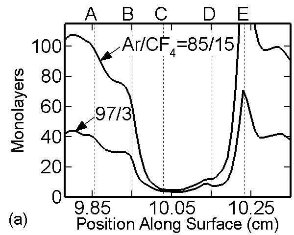
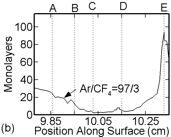
The number of layers of polymer deposited on the surface in and around the gap for a conventional focus ring is shown in Fig. 3a. This number decreases from about 40 for the Ar/CF4=97/3 mixture and 110 for the Ar/CF4=85/15 mixture on top of the wafer, to about 5 on the substrate under the gap. In fact, the deposition on the underside of the bevel is nearly 10 times more efficient than on the substrate under the gap due to the lack of ion sputtering, and so this difference is even more dramatic. For a high focus ring the number of layers of polymer on the surface after 20 seconds of processing is shown in Fig. 3b. Rings greater in height than the wafer are effective in reducing the amount of polymer deposited below the bevel.
|
|
| Fig. 3: Number of monolayers of polymer along the surface for a) convensional focus ring and (b) 2 mm focus ring height. Polymer deposition is disproportionately large in the gap due to the lack of ion sputtering. |
4. Ion Energy and Angular distribution
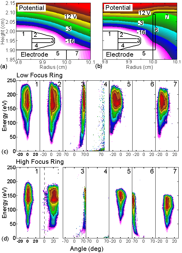
Plasma properties in the WFG with low (even with the wafer) and high (1 mm above the wafer) FRs for a 500 mm gap are shown in Fig. 4. The time averaged electric potentials are shown in Fig. 4a for the low FR and Fig. 4b for the high FR. The low FR allows the sheath to be more conformal to the bevel whereas the high FR maintains a more horizontally oriented sheath with an angle to the bevel. The resulting IEAD with the low FR on surface 1 (Fig. 4c) is skewed 5-10 degrees from the vertical, whereas that for the high FR (Fig. 4d) is nearly normal. These trends are opposite on the bevel (surface 2). The edge of the wafer (surface 3) with the low FR collects ion dominantly at 70 degrees and extending to 225 V. Lower energy ions are collected progressively closer to the normal during the anodic part of the cycle. The skew in the sheath edge with the low FR produces an IEAD to the substrate (surface 5) that is nearly 20 degrees from the normal whereas that with the high FR is centered about the normal. A similar trend occurs for the IEADs incident on the top of the edge of the FR (surface 7). Ion energies are lower by about 75 eV to surface 7 with the high FR due there being a voltage drop across the dielectric. Due to their vertically oriented inertia from acceleration in the upper part of the sheath, few ions are incident on the underside of the bevel (surface 4).
|
| Fig. 4. Plasma properties in the WFG with low and high FRs for a 500 mm gap. Time averaged electric potential with (a) low and (b) high FR. IEADs incident on different materials in the WFG with (c) low and (d) high FR. The numbers indicate the materials the ions strike. The IEADS for the high FR are generally more symmetric. |
*This work was supported by Applied Materials Inc. and the Semiconductor Research Corporation.
Last updated: June 11, 2009.